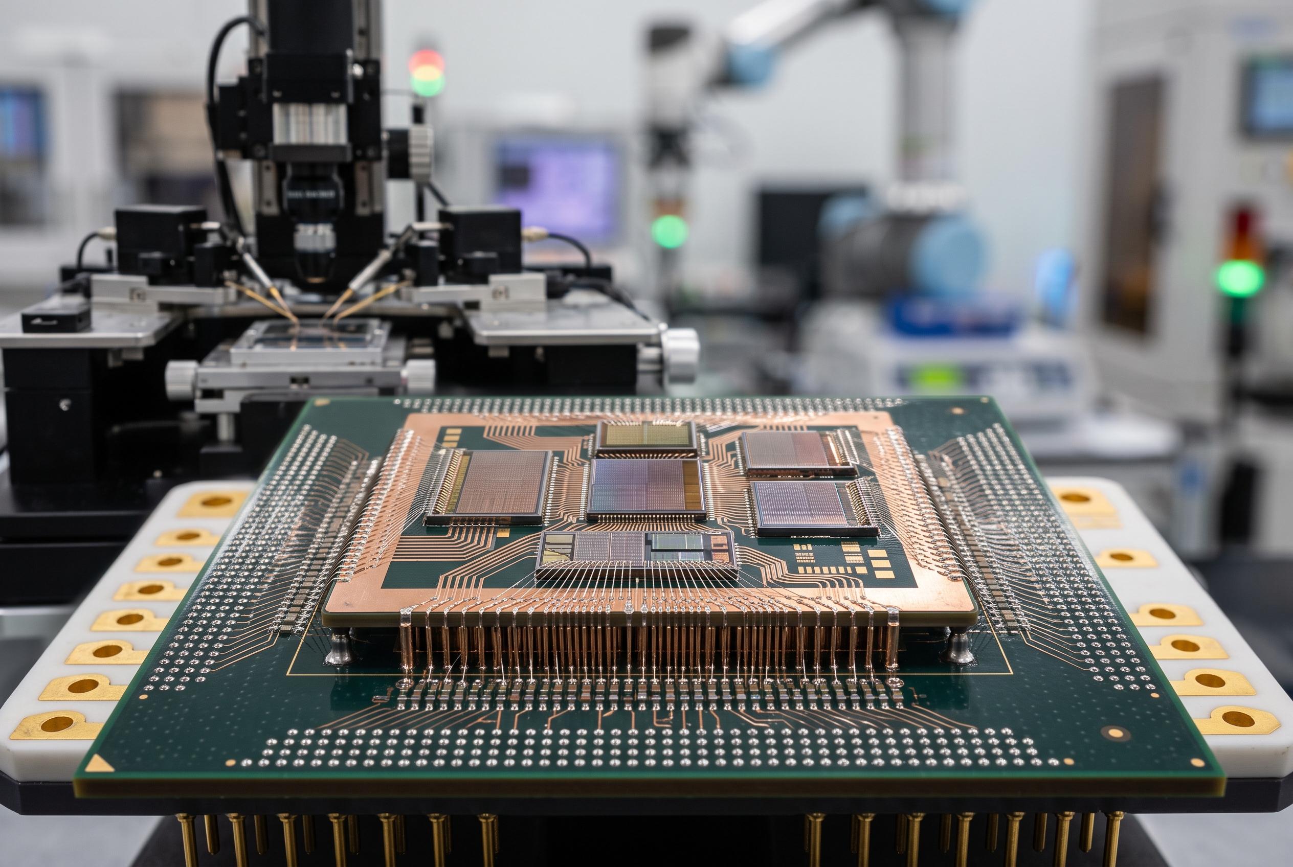

As foundry capacity tightens at TSMC, Intel’s innovative EMIB packaging technology attracts major technology firms like Broadcom, MediaTek, and Meta Platforms, signalling a shift in the competitive landscape for high-performance AI chips.
Intel’s advanced chip packaging business is drawing increasing attention from large technology groups as foundry capacity at TSMC remains tightly constrained, according to South Korean media cited by 3DNews. Broadcom, MediaTek and Meta Platforms are said to be among the companies now examining Intel’s services, with Google also reported to be involved through work on next-generation TPU designs. Intel has long argued that packaging can become profitable faster than wafer manufacturing, and the latest interest suggests that argument is gaining traction.
The appeal lies in Intel’s EMIB process, its 2.5D packaging approach for linking multiple dies within one package. Tom’s Hardware reported that EMIB is being viewed as a practical alternative to TSMC’s CoWoS method, which remains heavily booked. Intel says its packaging portfolio also includes EMIB-T, a variant that adds inter-layer connections to improve power delivery and signal routing for demanding AI chips. In Intel’s own product brief, the company says the technology is intended to support high-bandwidth, thermally efficient designs for artificial intelligence, machine learning and high-performance computing.
That capability matters because AI accelerators are growing larger and more complex, making advanced packaging a bottleneck in its own right. 3DNews said Intel’s EMIB can support combined chip assemblies with a total size far beyond the limits of a single monolithic die, with package dimensions reaching 120mm by 120mm. Intel has also suggested that packaging revenue should become a more meaningful part of its foundry business from the second half of next year, reflecting the company’s hope that demand for these services will accelerate before its wafer-side contract manufacturing does.
MediaTek in particular appears to be pursuing a multi-vendor strategy. According to reports cited by KuCoin and Technobezz, the company is using both Intel’s EMIB and TSMC’s CoWoS and SoIC services for AI ASIC and data centre chip development. That approach would give chip designers more flexibility as they navigate scarce advanced packaging capacity. For Intel, the broader implication is that packaging may prove to be one of the most commercially important parts of its foundry push, especially if major AI customers continue to diversify away from a single supplier.
Disclaimer: This content is intended for informational purposes only. Readers are advised to exercise their own judgement, conduct due diligence, or consult a qualified expert before acting on any information provided.