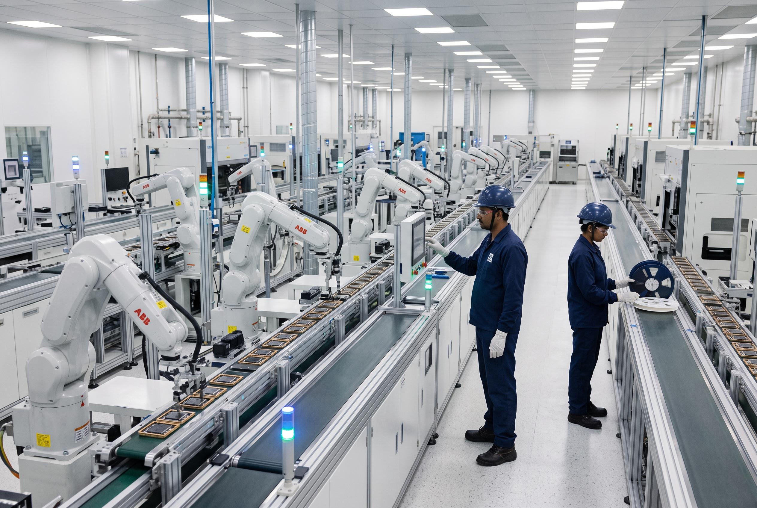

India ramps up its semiconductor strategy with a ₹1.27 trillion incentive package focused on mature nodes and assembly, aiming to capture a growing share of the global market and reduce reliance on China while supporting domestic demand.
India is making a second, larger push into semiconductors, this time with a sharper focus on mature chips rather than the most advanced ones. The aim is to win a meaningful share of the 28-nanometre and above segment, which powers cars, appliances, telecoms and internet of things devices and still accounts for most global chip volumes. According to Business Standard, the government believes this is where India can build scale more quickly, even as the US, Japan and South Korea shift their attention towards higher-margin leading-edge chips.
The latest step is Semicon 2.0, a ₹1.27 trillion incentive package approved by the Union Cabinet to support fabs, packaging plants, supply chains and chip design. The India Semiconductor Mission, which is implementing the country’s earlier ₹76,000 crore programme, is already backing projects across fabrication, assembly and packaging. Government material says the revised policy offers 50% fiscal support for eligible semiconductor projects, underlining how heavily the state is still relying on incentives to draw in capital and technology.
For now, India’s faster route is in outsourced semiconductor assembly and test, or OSAT, and in assembly, test, marking and packaging, known as ATMP. These plants are cheaper and quicker to build than full fabrication facilities, though they are also labour-intensive and carry lower margins. Business Standard reported that the first wave of approved OSAT and ATMP projects from Micron, Kaynes Technology, CG Power and Tata Electronics could together reach more than 70 million chips a day, while a second set of projects is also moving towards execution. The publication said the government wants India to capture 10% of the global OSAT and ATMP market by 2030.
That ambition is partly being driven by foreign customers looking to reduce exposure to China. Kaynes Semicon has said its capacity is already fully booked by clients in the US, Europe and Japan, while Suchi Semicon and Tata Electronics have also drawn overseas interest. Tata Electronics’ Dholera fab is being built with support from the semiconductor programme and is designed to make chips in the mature-node range. Tom’s Hardware reported that ASML has signed a memorandum of understanding with Tata Electronics to equip that plant, which is expected to have a capacity of 50,000 wafers a month.
India’s longer-term bet is that domestic demand will reinforce the industrial case. The electronics market is expanding, chip imports remain high and the Ministry of Electronics and Information Technology now estimates semiconductor demand could reach $150 billion by 2030. Even so, China remains the benchmark and the main rival: industry estimates cited by Business Standard suggest it will keep dominating mature-node production, while India’s first fab will not come on stream until about 2028. For the moment, the country’s semiconductor strategy is less a claim of victory than a statement of intent: to become a credible alternative in a market that values supply security as much as cost.
Disclaimer: This content is intended for informational purposes only. Readers are advised to exercise their own judgement, conduct due diligence, or consult a qualified expert before acting on any information provided.