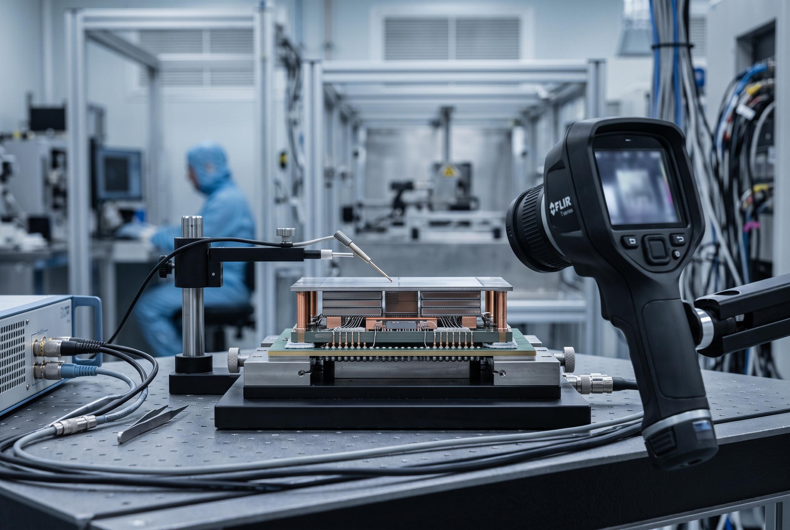

The semiconductor industry is moving towards larger, more complex multi-die packages driven by physical limits, thermal management challenges, and rising performance demands, fundamentally transforming chip design and manufacturing strategies.
The semiconductor industry is moving towards a new default: multi-die assemblies, not single large chips, will do more of the heavy lifting for AI-era computing. According to SemiEngineering, that shift is being driven by the limits of reticle-sized dies and by the need to combine CPUs, GPUs, accelerators, memory and specialist logic in one package. Tom’s Hardware has also reported that TSMC is exploring a 1,000W-class multi-chiplet processor built around CoWoS, a sign of how far package-level integration is being pushed to meet extreme performance targets.
That transition is changing both architecture and economics. The old model of simply shrinking logic to gain performance is running into physical and financial limits, while the rise of agentic AI is adding more orchestration complexity to workloads that already strain data-centre systems. The IEEE International Roadmap for Devices and Systems, established in 2016 after the earlier ITRS effort ended, reflects how broadly the industry now thinks about these problems, spanning packaging, materials, lithography and system design rather than transistors alone. SemiEngineering’s reporting also shows that design teams increasingly need simulation and AI tools simply to validate whether a chiplet mix will be manufacturable and useful by the time it reaches integration.
Packaging is now as important as transistor scaling. Intel’s EMIB bridge technology has already been in volume production for years, showing that high-density die-to-die connections are no longer experimental. At the same time, the industry is exploring larger interposers, redistribution-layer fan-out, glass, and organic substrates as ways to reduce cost or improve performance. Tom’s Hardware has reported that Rapidus is pursuing panel-level packaging on glass substrates, underlining the growing interest in materials with better dimensional stability and thermal behaviour.
Thermal management is becoming one of the hardest constraints. As more compute is packed into one module and utilisation rises in large servers, air cooling is often no longer enough. SemiEngineering describes a growing menu of approaches, from liquid cooling and cold plates to microchannels, immersion and two-phase systems. MIT Lincoln Laboratory’s work on an active wafer-scale reconfigurable logic fabric, which includes integrated cooling, points to the same conclusion: bandwidth, latency and heat must be solved together, not separately.
There is also renewed interest in new stacking models. IBM Research has described a hybrid “nanostack” approach that uses angled transistor stacking and fewer routing tracks, with the company saying it could improve performance, energy efficiency and SRAM density. That sort of architecture suggests that the next gains will not come only from smaller features, but from closer co-design of layout, materials, thermal paths and mechanical stability. For leading-edge nodes at 2nm and below, that co-ordination is becoming essential rather than optional.
The broader implication is that chipmaking is becoming a systems problem at every level. Custom chiplets may remain the best answer for very high-value workloads, but they are expensive and difficult to standardise, which is why large cloud firms and automotive groups are still testing the limits of reuse. What is clear from the latest industry work is that the future of advanced semiconductors will depend on packages that are larger, more heterogeneous and far more computationally intensive to design, simulate and manufacture than the single-die era ever required.
Disclaimer: This content is intended for informational purposes only. Readers are advised to exercise their own judgement, conduct due diligence, or consult a qualified expert before acting on any information provided.