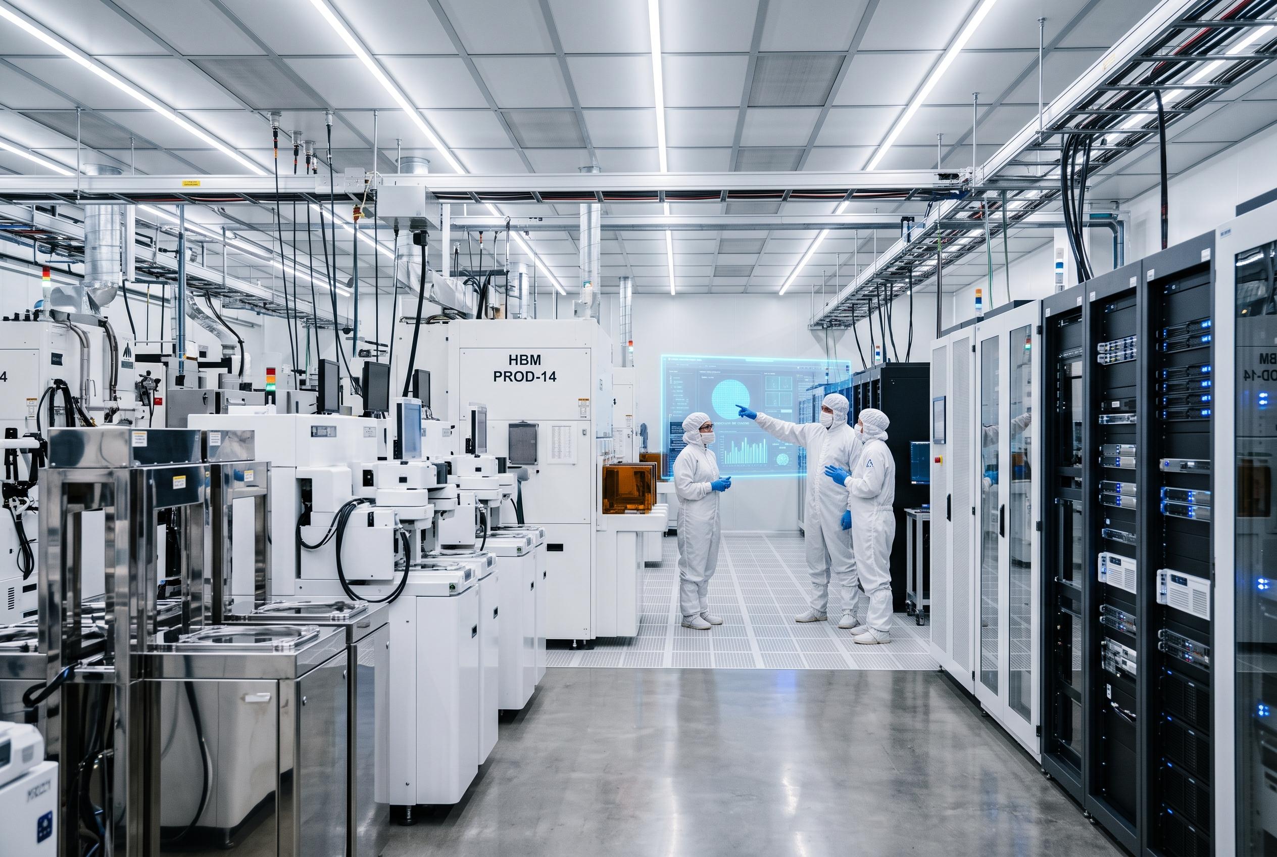

Samsung is contemplating shifting its legacy DRAM and NAND packaging work from South Korea to Vietnam to focus its Korean sites on high-bandwidth memory, responding to rising AI memory demand and capacity constraints.
Samsung Electronics is weighing whether to shift packaging and testing work for standard DRAM and NAND flash from its Cheonan and Onyang backend sites in South Korea to Vietnam, according to reports citing Korean industry sources. The move would free up floor space and specialist equipment for high-bandwidth memory stacking, which has become the company’s most pressing manufacturing priority as demand for AI memory keeps rising. The consideration comes as Samsung targets a 47% increase in HBM wafer output by the end of 2026 and reports that its sixth-generation HBM4 yield has already reached about 80%. The company has not confirmed the plan publicly.
The logic is largely one of process separation. Conventional memory packaging and HBM stacking use different equipment, different materials and different production flows, making it difficult to run both on the same cleanroom lines. Samsung has already acknowledged that Cheonan is effectively full for HBM stacking, while Onyang’s new backend building was designed specifically for that work. Industry reports suggest the company is now considering a two-track structure: moving commodity DRAM and NAND packaging out of South Korea while concentrating HBM backend capacity at its Korean sites.
Vietnam would be a natural destination for that work because Samsung already has a large manufacturing base there. The company operates multiple factories, an R&D centre and a sales operation across Bac Ninh, Thai Nguyen, Hanoi and Ho Chi Minh City, and it is already the country’s biggest foreign investor with committed spending of more than $23 billion. Earlier this year, Samsung also outlined plans for its first semiconductor test plant in Thai Nguyen Province, a $1.5 billion project expected to begin operations in November 2027 and focused on legacy DRAM and NAND validation.
That investment matters because Samsung has been steadily building the backend infrastructure needed for older memory products outside South Korea. Vietnam already hosts semiconductor assembly, packaging and testing operations from Intel, Amkor Technology and Hana Micron, which gives Samsung a supply-chain and labour base for transferring mature memory work. In practice, that would allow the company to reserve its Korean facilities for HBM, where throughput is more valuable and harder to expand.
The strategic pressure is clear. According to Samsung’s February launch, HBM4 entered mass production with a sustained data rate of 11.7 gigabits per second per pin, making it suitable for Nvidia’s next-generation AI platforms. Reuters and industry analysts have reported that Samsung, SK hynix and Micron all completed qualification for HBM4, but Samsung is still working to convert better yields into higher shipment volumes. With HBM demand expected to stay tight through 2027, backend capacity has become the limiting factor, not wafer output alone.
Samsung’s wider memory strategy points in the same direction. The company has already cut back on commodity memory lines, including MLC NAND and older LPDDR products, as it shifts resources towards higher-margin AI memory. If the Vietnam transfer proceeds, it would be another sign that Samsung is reorganising its manufacturing footprint around a simple priority: more space, more equipment and more labour for HBM, and less for legacy chips.
Disclaimer: This content is intended for informational purposes only. Readers are advised to exercise their own judgement, conduct due diligence, or consult a qualified expert before acting on any information provided.