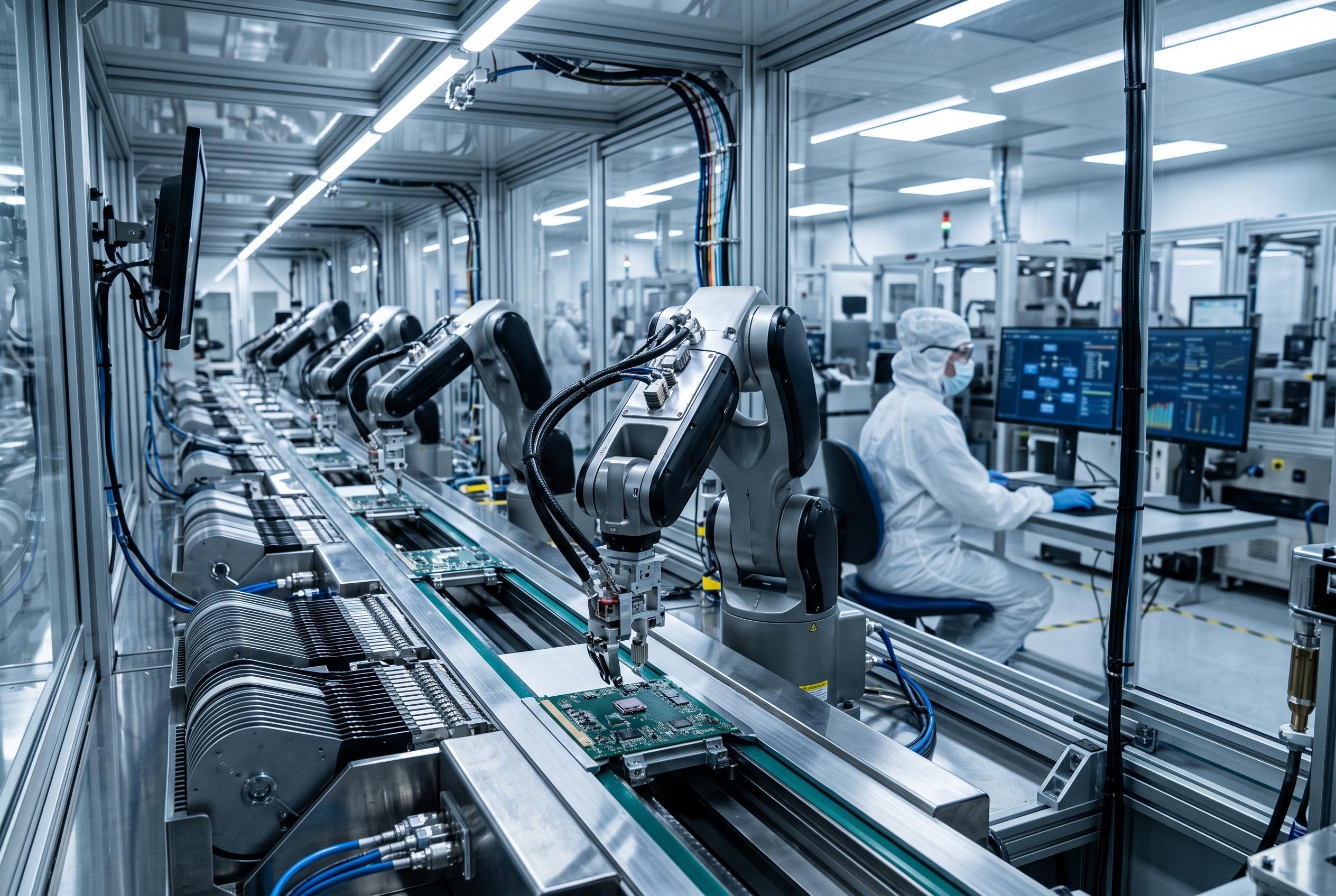

India’s semiconductor packaging sector is transitioning from policy promises to tangible factory developments, with the launch of its first high-end outsourced plant in Visakhapatnam, signalling a key step in building a domestic backend ecosystem aligned with global standards.
India’s semiconductor packaging build-out is beginning to move from policy intent to factory floors. In Visakhapatnam, Hyderabad-based Advanced System in Package Technologies has started work on an outsourced semiconductor assembly and test plant with South Korea’s APACT, a project the company says should reach production within 18 months. The Andhra Pradesh government approved the facility at ₹2,500 crore, and the broader plan is part of India Semiconductor Mission 1.0, which has backed nine packaging projects spanning memory assembly, legacy packages, power devices, flip-chip lines and the first stages of advanced packaging.
The ASIP site is being positioned as a stepping stone rather than a pure legacy-packaging plant. According to the company, initial output will centre on flip-chip ball-grid array and wire-bond packages, while 2.5D packaging is being targeted for 2030. ASIP chief executive Venkata Simhadri told EE Times that the company expects the building and cleanroom shell to be completed within about a year, followed by equipment installation, trial runs and qualification before full-scale output begins. The timeline is ambitious, but it reflects the urgency now surrounding India’s attempt to build a domestic backend ecosystem.
That effort is not limited to one company. India’s packaging push already includes projects from Micron, Tata Semiconductor Assembly and Test, CG Power’s CG Semi unit, Kaynes Semicon, 3D Glass Solutions, Continental Device India, SiCSem and Suchi Semicon. The mix matters because these facilities are not all pursuing the same market. Micron is focused on memory, CG Semi is building on more established package types, Kaynes is targeting power applications, and Tata, CG Semi and Kaynes are also developing flip-chip capabilities. The result is an ecosystem that is still broad rather than deep, but one that is beginning to cover both legacy and more demanding package classes.
APACT’s role also illustrates a key feature of the current Indian strategy: imported know-how remains central. The Korean company, which was spun out of SK Hynix and has experience in DRAM, multi-die stacking and system-in-package work, is bringing process expertise to a market where advanced packaging skills are still limited. Simhadri said the partnership is the first of its kind between a Korean and an Indian semiconductor company. He also said ASIP approached several Korean and Taiwanese OSATs before settling on APACT, underlining how dependent the sector remains on external expertise, equipment and, in some cases, existing customer relationships.
The domestic market, however, is not starting from zero. Wasi Uddin, formerly a consultant on OSAT and ATMP at MeitY and now a senior manager at Kaynes, told EE Times that packaging had existed in India before ISM 1.0, but only at a very small scale. He said the mission’s $10 billion framework was designed to pull in more serious manufacturing capacity. The projects approved under it are aimed at a wide range of end uses, including automotive, consumer electronics, healthcare and industrial systems. In practice, that means much of the near-term demand will still be for conventional packages, even as a smaller number of lines move towards flip-chip and, eventually, chiplet-oriented designs.
The technical hurdle for that next step is substantial. Uddin said India still needs to strengthen precise flip-chip alignment, redistribution layers and interposer technology before it can package AI accelerators, chiplets and high-performance computing devices at scale. He described the missing capabilities as the basis for more advanced 3D and 2.5D assembly, as well as for system-in-package integration that combines multiple dies and components in one module. ASIP says it is already discussing 2.5D with customers and partners, while Simhadri insists the company will not wait for the new plant to be finished before developing that roadmap. Whether India can turn these plans into reliable production will depend not just on factory construction, but on the slower work of training engineers, qualifying suppliers and building the process discipline that semiconductor packaging demands.
Disclaimer: This content is intended for informational purposes only. Readers are advised to exercise their own judgement, conduct due diligence, or consult a qualified expert before acting on any information provided.