

Applied Materials has opened a 600,000-square-foot research hub in California, bringing chipmakers, equipment suppliers and universities together to speed the development of AI-era manufacturing processes.
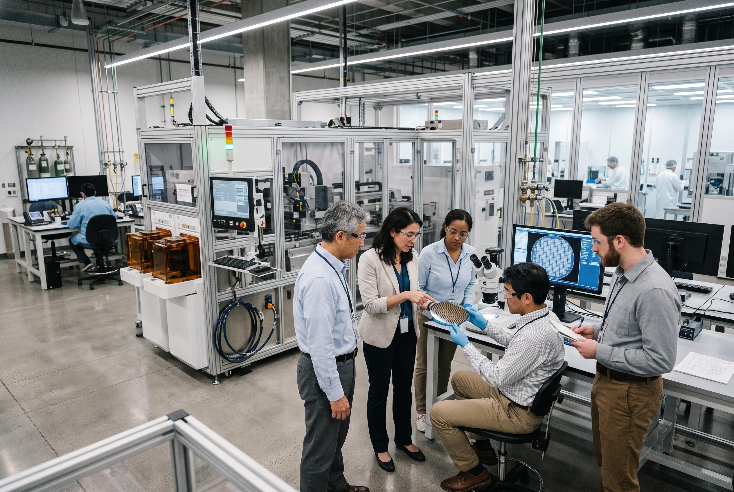
Applied Materials has opened what it says is the world’s largest facility dedicated to collaborative semiconductor process technology and manufacturing equipment research, placing a major bet on the part of the chip supply chain that usually remains out of sight. The EPIC Centre in Sunnyvale, California, spans 600,000 square feet and includes nearly four acres of cleanroom space. The company has described it as a $5 billion capital investment designed to shorten the journey from laboratory concept to commercial manufacturing for the AI era.
That wager matters because the bottleneck in AI computing is no longer limited to the accelerator itself. Advanced memory stacks, packaging, backside power delivery and other device structures depend on manufacturing steps that must be executed with atom-level precision. According to Applied Materials, EPIC is intended to bring chipmakers, systems companies, equipment suppliers and university researchers into a shared environment so that new process flows can be developed and validated earlier, before they reach a customer’s factory.
The logic behind the project is that semiconductor transitions take far longer than product cycles in AI. Applied says the centre is meant to compress the gap between invention and high-volume production by letting customers work on next-generation equipment years before it would normally enter a fab. The company has also said, in its own announcement, that this is the first time chipmakers can have dedicated space inside an equipment maker’s research facility, giving them earlier access to new processes and tools.
Applied is not building the programme alone. Its public materials identify founding partners including TSMC, Intel, Samsung, Micron and SK hynix, alongside companies such as Broadcom, Advantest, SCREEN, KIOXIA and Besi, plus research partners at Arizona State University, Rensselaer Polytechnic Institute, Stanford, UC Berkeley and UCLA. The addition of ASU, RPI and Stanford underscores the company’s effort to reinforce the U.S. lab-to-fab pipeline and train engineers in manufacturing-relevant environments, rather than leaving academia and production as separate worlds.
For the broader AI infrastructure market, the significance is practical. If process development moves faster, suppliers can potentially deliver more efficient chips and packaging sooner, improving performance per watt and easing some supply constraints. Applied is also signalling where semiconductor value creation may be shifting: towards the companies that help determine what can actually be manufactured at scale, not only those that sell the tools on which manufacturing depends. Its newly introduced chipmaking systems, including Kinex, Centura Xtera and PROVision 10, reinforce that push towards what the company calls the angstrom era of chipmaking, where atomic-level control becomes central to both logic and advanced packaging.
The real test will be whether EPIC produces demonstrable gains in time to yield and time to volume, not just a larger footprint and a long list of partners. If it does, the centre could become an important lever for the next wave of AI hardware, where the limiting factor is increasingly the speed at which materials science can be turned into manufacturable reality.
Disclaimer: This content is intended for informational purposes only. Readers are advised to exercise their own judgement, conduct due diligence, or consult a qualified expert before acting on any information provided.