

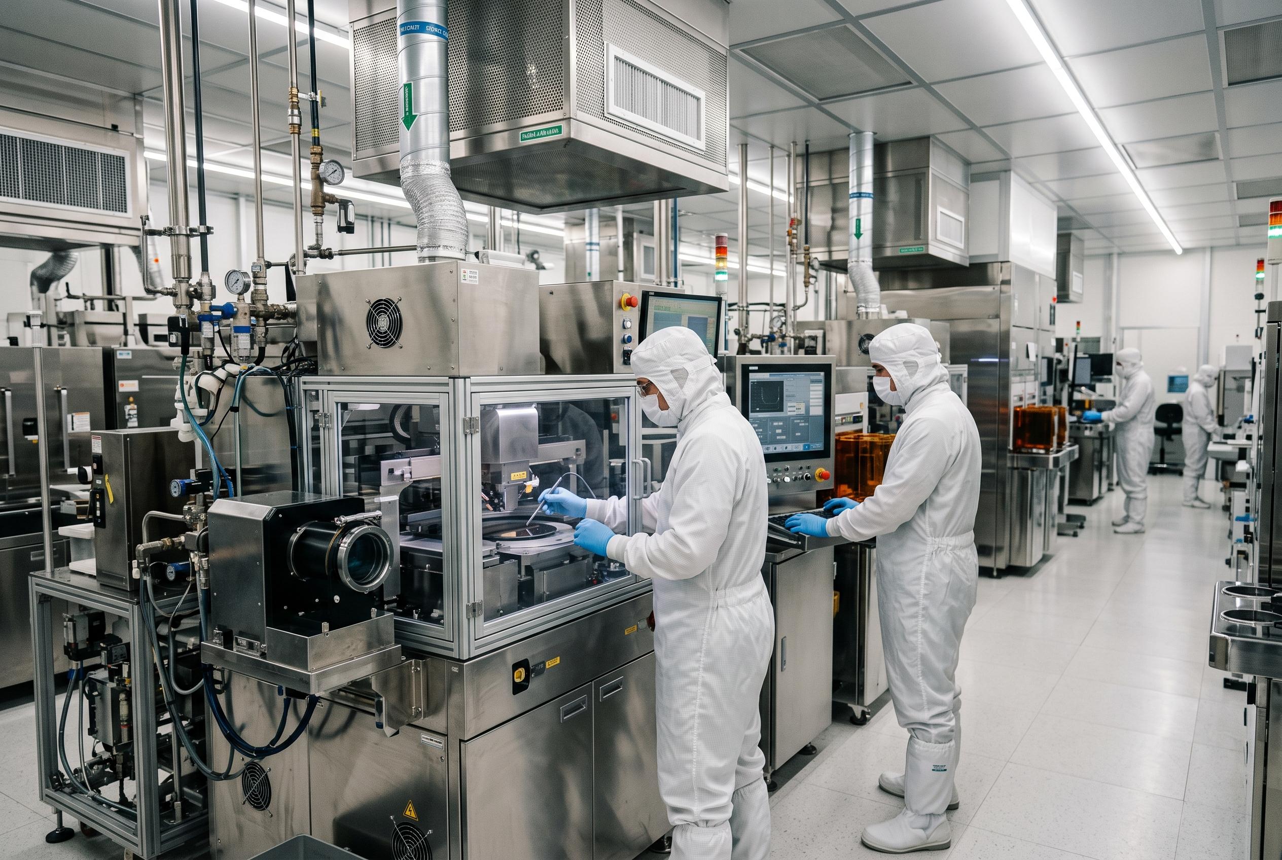

Tata Electronics’ Gujarat foundry has attracted six prospective customers, but delayed production, rising losses and uncertain volumes mean its commercial success will depend on qualification, yields and repeat orders.
Tata Electronics’ planned Dholera fab is moving from the announcement stage into a harder commercial test: whether early customer interest can be turned into steady wafer output. According to the material released by the project, the India-based venture with Taiwan’s PSMC is being built as a 300mm foundry in Gujarat with a target capacity of up to 50,000 wafers a month, aimed at mature-node production for power-management chips, display drivers, microcontrollers and other logic products. The company says the facility is designed for 28nm to 110nm technologies, although related industry summaries indicate the first production is more likely to begin at 55nm and 90nm before moving to more advanced mature nodes.
That commercial ramp is still some distance away. Multiple reports say the fab remains under construction, with trial output expected late this year and full production now pushed to mid-2028. One industry guide says the project received Union Cabinet approval on 29 February 2024 under the India Semiconductor Mission, and a fiscal support agreement followed on 5 March 2025. Tata Electronics has also said the foundry will offer design support, verified electronic design automation tools and cloud-based design environments, signalling an effort to secure customers before the plant begins shipping wafers.
The more immediate challenge is not construction, but qualification. DigiTimes reported that Tata has six customers engaged with the Dholera project, including three with binding offtake commitments, one with a capacity reservation and two in early-stage discussions, but the company has not disclosed volumes or contract terms. Analysts cited in the report said the project’s success will depend on yields, utilisation, repeat orders and the ability to convert reservations into recurring wafer starts, rather than on headline commitments alone.
That concern is sharpened by internal pressure over capital allocation. According to the same round-up, Tata Trusts chairman Noel Tata is said to favour faster returns on investment, while Tata Sons chairman Natarajan Chandrasekaran is arguing that the semiconductor business needs patience. The report said Tata Electronics’ revenue almost doubled in fiscal 2026, but losses widened, and cumulative investment by Tata Sons had reached Rs99.61 billion. That combination of rising spending and delayed revenues underlines how long fabrication projects can remain cash-heavy before any meaningful payoff arrives.
The Dholera project also sits within a wider regional push to deepen semiconductor manufacturing capacity for artificial intelligence and industrial electronics. Micron has opened a second advanced assembly and test site in Taiwan, while TSMC has won Japanese approval for revised Kumamoto plans that shift one plant towards 3nm output and preserve long-term supply commitments to domestic customers. In that context, Tata’s fab is part of a broader competition to secure packaging, mature-node capacity and supply-chain resilience, but its eventual value will depend on execution as much as on policy support.
Disclaimer: This content is intended for informational purposes only. Readers are advised to exercise their own judgement, conduct due diligence, or consult a qualified expert before acting on any information provided.