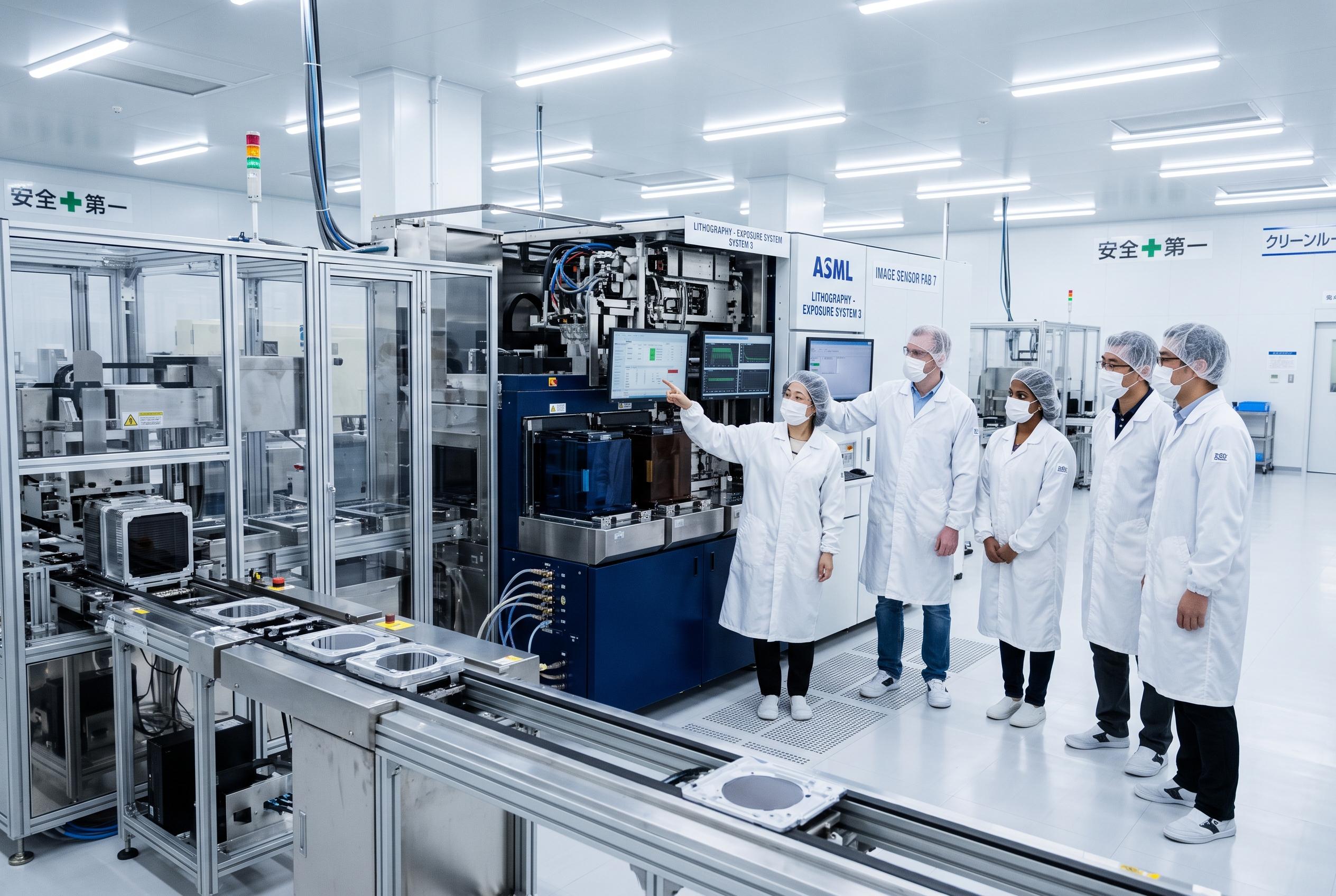

Sony Semiconductor Solutions and Taiwan Semiconductor Manufacturing Co. announce a joint venture to co-develop advanced image sensors at Sony’s new Kumamoto facility, marking a shift towards a ‘fab-light’ model amid rising global competition in sensor technology.
Sony Semiconductor Solutions and Taiwan Semiconductor Manufacturing Co. said they plan to create a joint venture to develop and manufacture next-generation image sensors at Sony’s new facility in Koshi City, Kumamoto Prefecture. The companies said the project is aimed at applications in physical AI, including automotive systems and robotics, and that Sony will hold a majority stake. The move would give Sony a more open manufacturing model for a business that has long been built on in-house design and production.
For Sony, the arrangement marks a notable break from a vertically integrated approach that had defined its sensor business for decades. The company has traditionally designed the devices, refined the manufacturing process and built the chips itself in Japan. By contrast, the new plan shifts part of that burden to TSMC, which brings advanced process technology and high-volume foundry expertise. That is why Sony has described the proposal as a move towards a “fab-light” structure, while retaining control of sensor design and key intellectual property.
The technical logic is straightforward. Modern stacked CMOS image sensors separate the light-sensitive pixel layer from the logic layer that handles signal processing and, increasingly, AI-related computation. Sony’s strength lies in the pixel architecture, while TSMC’s core advantage is producing advanced logic at smaller process nodes. In practical terms, that matters because automotive and robotics systems need sensors that can process data quickly, use less power and cope with difficult lighting conditions in real time. The companies said the partnership is intended to combine those strengths in a single manufacturing environment.
The investment also reinforces Kumamoto’s role in Japan’s semiconductor strategy. Sony has already been building the Koshi plant with support from the Japanese government, which approved subsidies earlier this year under an economic security framework. According to the company’s earlier disclosure, the facility is expected to be capable of producing 10,000 300-millimetre wafers a month, with production targeted for May 2029. The joint venture’s output is also expected to begin around 2029, although the final terms still need to be settled and the project remains subject to formal agreements.
The timing comes as competition in image sensors intensifies. Samsung won a deal late last year to supply Apple with stacked image sensors, ending Sony’s long-standing dominance in that account. Sony’s global share of the image sensor market has also eased from earlier highs, while Samsung and China’s OmniVision have been pushing harder into both smartphone and automotive chips. Against that backdrop, the Sony-TSMC venture looks both defensive and strategic: defensive in protecting Sony’s lead, and strategic in pushing deeper into markets where sensor performance is becoming a central constraint on next-generation AI systems.
Disclaimer: This content is intended for informational purposes only. Readers are advised to exercise their own judgement, conduct due diligence, or consult a qualified expert before acting on any information provided.