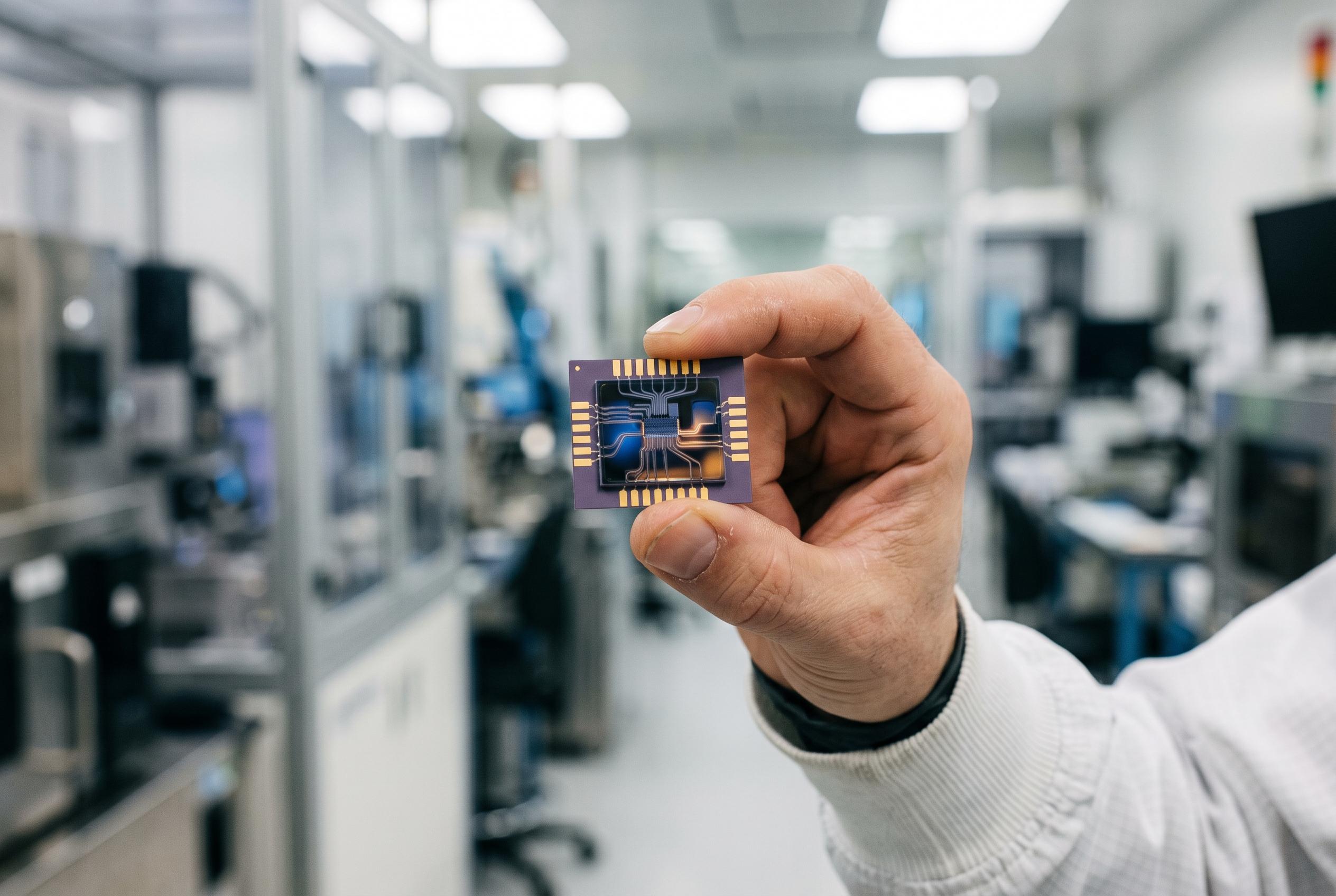

Researchers leverage AI algorithms to drastically reduce the size of key photonic chip components, paving the way for more compact and efficient optical systems in communications and quantum computing.
Artificial intelligence is beginning to change how photonic microchips are designed, with researchers using an inverse-design algorithm to shrink three key components by as much as 500 times. According to reports from XenoSpectrum and Live Science, the work was led by teams at the Max Planck Institute for the Science of Light and Harvard SEAS, and the findings were published in Nature Communications on 28 May 2026.
Photonic chips use light, rather than electrons, to move and process information. That makes them attractive for fibre-optic communications, data centres, artificial intelligence systems, lidar and quantum computing because they can offer higher speed, greater bandwidth and lower heat loss. The latest advance matters because it frees physical space on the chip for other functions, which is a major constraint in compact optical systems.
Instead of refining an existing layout, the researchers told the algorithm what each part needed to do and what manufacturing limits had to be respected. The system then tested thousands of possible structures before settling on designs that could control light effectively. The components produced were a wavelength demultiplexer, a spatial mode demultiplexer and mirrors for steering light. Live Science reported that the mirror, just 11 micrometres long, reflected 98.5% of incoming light, while XenoSpectrum said the mirrors allowed light to bounce more than 100 times before fading.
The parts were fabricated in thick silicon nitride, measured at roughly 400 to 800 nanometres, to reduce optical loss and improve wavelength control. For now, the devices have been shown separately rather than in a single working circuit, so integration remains the next step. Even so, the result suggests AI can generate production-ready photonic layouts that go beyond conventional engineering intuition, a point echoed in later coverage that described the designs as unusually compact yet practical to manufacture.
Disclaimer: This content is intended for informational purposes only. Readers are advised to exercise their own judgement, conduct due diligence, or consult a qualified expert before acting on any information provided.