

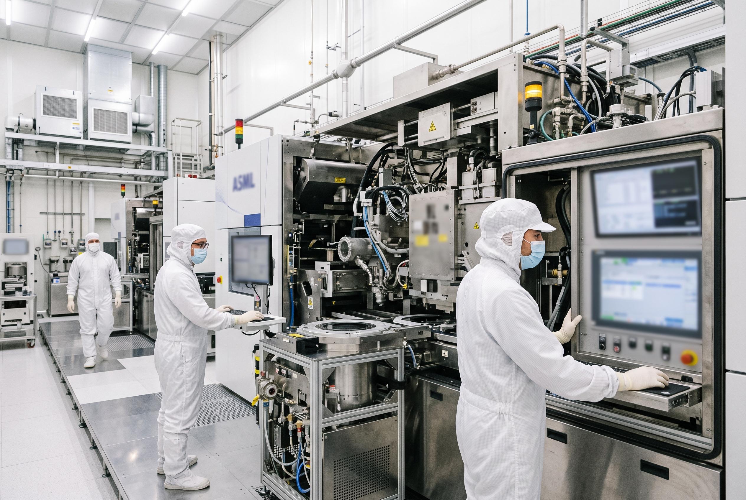

ASML and Carl Zeiss say a feasibility-stage Hyper NA system could pattern features as small as 5 nanometres in the 2030s, reusing much of today’s EUV technology.
ASML and its German optics supplier Carl Zeiss have sketched a possible successor to the Dutch company’s most advanced chipmaking platform, saying a so-called “Hyper NA” system could be ready in roughly a decade. In a peer-reviewed paper, engineers said the concept would build on much of the existing extreme ultraviolet, or EUV, architecture while pushing chip features smaller still. The work suggests the next leap in lithography may come not from a wholly new machine, but from a more exacting version of the technology that already underpins the most advanced semiconductors.
The proposal matters because ASML sits at the centre of the chip industry’s effort to shrink transistors and raise performance without increasing power use. According to the paper in the October issue of the Journal of Micro/Nanopatterning, Materials and Metrology, Hyper NA could pattern features as small as 5 nanometres, which would be more than a third smaller than the company’s current High NA EUV tool. Even as chipmakers adopt more three-dimensional designs, lithography remains a limiting factor, and finer patterning is still crucial for the fastest and most power-efficient chips.
The roadmap also shows how much of the current platform might be reused. The authors said Zeiss already has mirrors precise enough for the proposed tool and that the machine would be only slightly larger than High NA systems, which are already as large as a double-decker bus. They added that ASML’s present light source could be used without modification. At the same time, they noted that further gains beyond Hyper NA would probably require shorter wavelengths, an area still largely confined to academic research.
That future is not yet settled, however. ASML has begun work on the concept but has not committed to producing it, and the company declined to comment immediately, according to the report. Tom’s Hardware said the concept is still in feasibility studies for the 2030s and that major technology and cost hurdles remain. The timing matters for chipmakers as well: Intel has already started using High NA in production, while Samsung and SK Hynix have said they intend to follow in 2028 and TSMC in 2030. The discussion is also relevant to US start-ups such as xLight, which is developing free-electron laser light sources, and Substrate, which is pursuing X-ray lithography, because the paper’s note on light-source reuse suggests ASML’s next step may not require a wholesale redesign of the illumination system.
Disclaimer: This content is intended for informational purposes only. Readers are advised to exercise their own judgement, conduct due diligence, or consult a qualified expert before acting on any information provided.