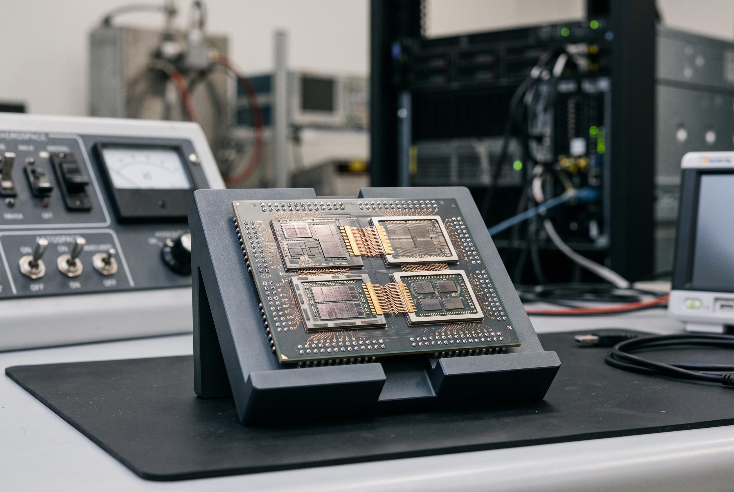

Semiconductor manufacturers are increasingly adopting chiplet-based designs enhanced by the UCIe 1.1 standard, enabling faster, more efficient systems in aerospace, defence, and AI applications, with new innovations expected to shape the future of high-speed interconnects and integration.
The move towards chiplet-based design is accelerating as semiconductor makers look for ways to manage heat, routing complexity and power use in demanding systems. In aerospace, defence, telecommunications and high-performance computing, modular packaging is increasingly preferred over large monolithic dies because it allows different functions to be built on the most suitable process and then combined in one package. According to the lead report, one of the most significant developments in this area is the direct integration of the UCIe 1.1 interconnect standard into adaptive system-on-chip architectures.
By placing the die-to-die link inside the package rather than relying on board-level serial connections, designers can cut parasitic effects, reduce loss and lower energy use. The report says the architecture can support up to four UCIe standard-package links and up to two advanced-package links, creating aggregate bandwidth in the multi-terabit-per-second range. That kind of connectivity matters most where data must move quickly between compute, memory, radio-frequency and optical components without the penalties of external traces.
The broader importance of UCIe 1.1 is that it strengthens the chiplet model for high-reliability and mixed-signal systems. Phoronix reported that the specification adds runtime health monitoring and repair, support for simultaneous multiprotocol operation with full link-layer functionality for streaming protocols, and new bump maps intended to reduce packaging cost. It is also fully backward compatible with UCIe 1.0, which should ease adoption in existing ecosystems.
The technical appeal is clearest in applications that need disparate silicon technologies to work together. The report highlights RF front ends, optical co-packaged networking and AI acceleration, where a single process node is rarely optimal for every block. The adaptive devices described combine multi-channel RF data converters, programmable logic, hardened DSP blocks and AI engines claimed to deliver up to 80 TOPS. By using UCIe-compliant links, the package can integrate third-party ASICs, CPUs, GPUs and optical modules, with the stated aim of reducing size, weight, power and cost. Initial production silicon is slated for the fourth quarter of 2027.
Disclaimer: This content is intended for informational purposes only. Readers are advised to exercise their own judgement, conduct due diligence, or consult a qualified expert before acting on any information provided.