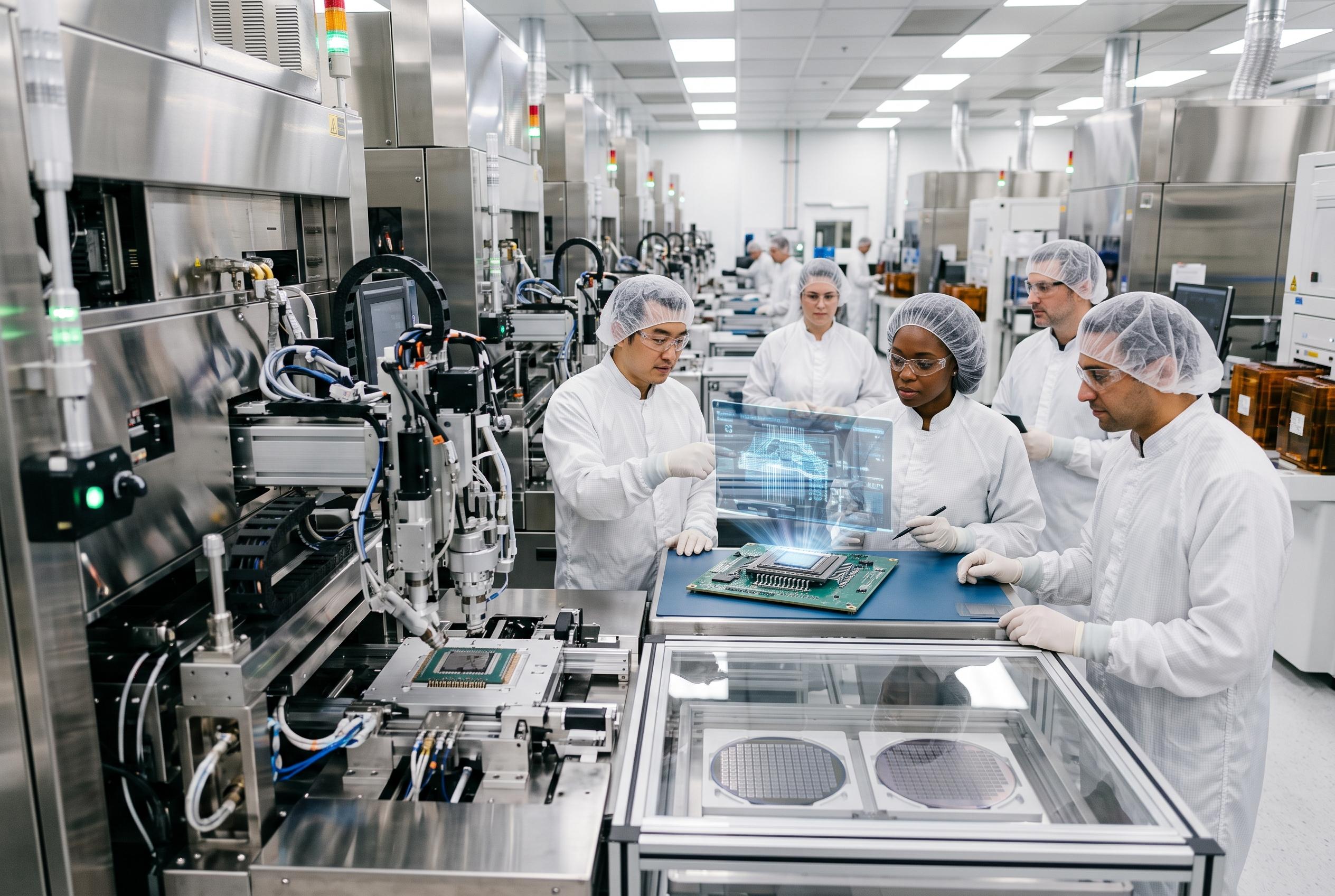

Taiwanese foundry TSMC is ramping up its CoWoS capacity significantly, aiming for a doubling by 2028 to address soaring AI chip requirements, with strategic investments in Arizona and Taiwan amid supply chain pressures.
TSMC is preparing a much larger push into advanced chip packaging as AI demand continues to strain supply chains. According to UDN, analysts believe the Taiwanese foundry wants CoWoS capacity to reach 130,000 wafers a month by the end of this year and 260,000 by the end of 2028, roughly doubling output over that period. The expansion would centre on the company’s Arizona site and its AP7 plant in Taiwan.
CoWoS has become one of the most important bottlenecks in the AI chip market because it links logic and memory dies through a dense silicon interposer. That design is particularly well suited to high-bandwidth accelerators from Nvidia and other AI customers. By contrast, Intel’s EMIB-T uses bridges embedded in an organic substrate rather than a full interposer, a different approach that supply-chain reports say is gaining interest as customers look for more packaging options.
TSMC’s wider business remains under heavy pressure from the AI boom. PC Gamer reported that the company posted record revenue of about $16.35 billion in August 2026, its fourth straight monthly high, while retaining a dominant share of the global foundry market. The same demand has left leading-edge process lines effectively full, which helps explain why packaging capacity has become as strategically important as wafer fabrication itself.
That scarcity is also encouraging customers to diversify. Tom’s Hardware reported that OpenAI has indicated future processors could be made at Samsung as well as TSMC, suggesting large-volume requirements that may be difficult for one foundry to absorb alone. Taiwanese analysts quoted in the supply-chain reporting also say the shortage of CoWoS has lifted demand for packaging work from firms such as Amkor, UMC and ASE, while EMIB-T could emerge as a meaningful alternative for custom AI silicon from companies including Google and Amazon.
Looking further ahead, TSMC is also planning for the next generation of manufacturing tools. Tom’s Hardware reported that the company expects to start high-volume use of High-NA EUV lithography in 2030, with A10 or A11 among the likely first nodes. That points to a longer-term effort to keep pace with increasingly complex chip designs even as packaging, rather than transistor scaling alone, becomes the main battleground in AI semiconductors.
Disclaimer: This content is intended for informational purposes only. Readers are advised to exercise their own judgement, conduct due diligence, or consult a qualified expert before acting on any information provided.