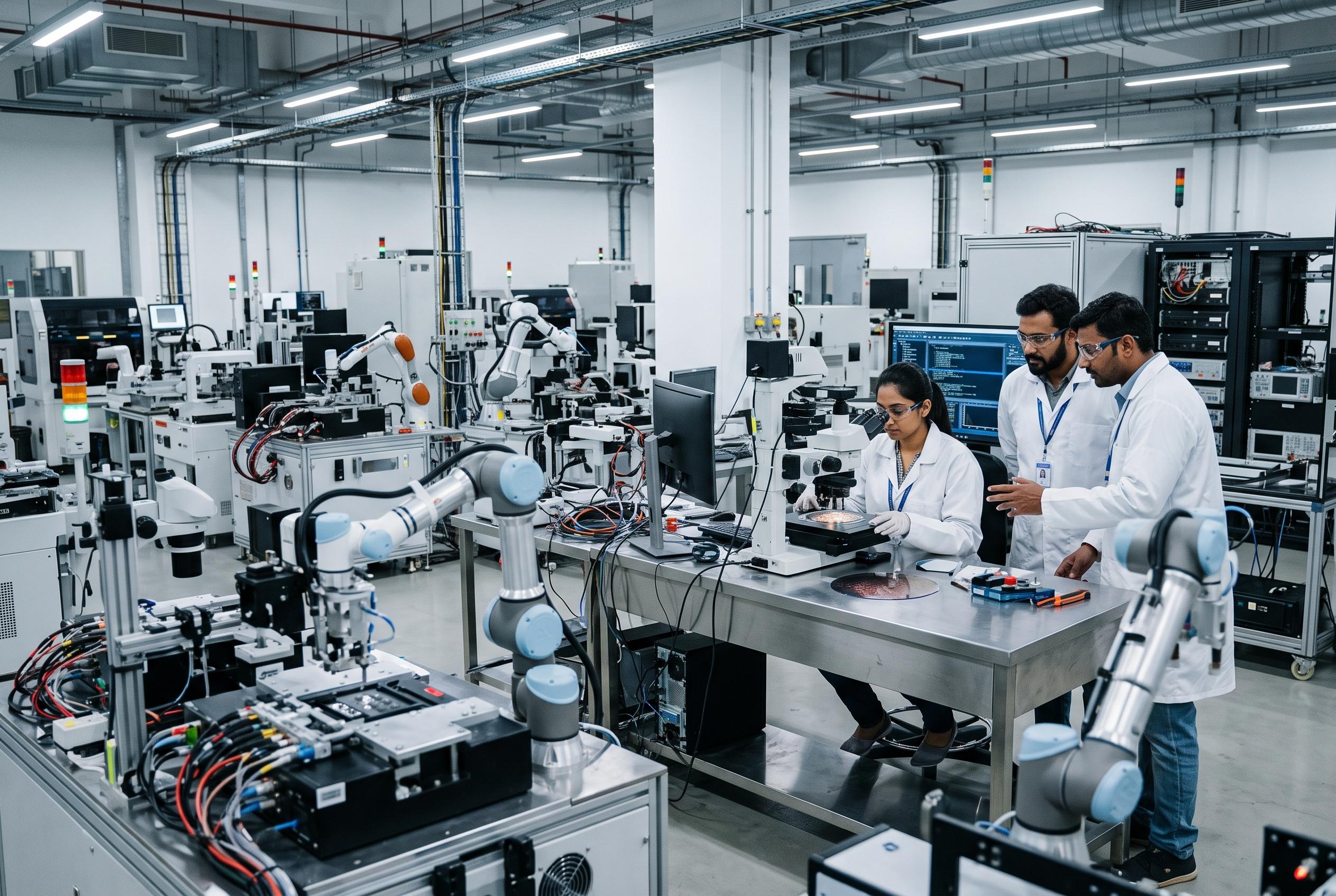

HCLTech has inaugurated a ₹185 crore, 40,000 sq ft semiconductor laboratory in Bengaluru, enhancing India’s post-silicon engineering capabilities and supporting the nation’s push to move beyond chip design into more complex manufacturing processes.
HCLTech has opened a ₹185 crore advanced semiconductor laboratory in Bengaluru, a move that adds fresh capacity to India’s chip engineering base at a time when the country is trying to expand beyond design work into more of the value chain. The company said the 40,000 sq ft facility is built for post-silicon engineering, advanced testing and failure analysis, functions that help confirm whether a chip performs as intended after fabrication and before large-scale deployment.
The lab includes 25,000 sq ft of Class 10K and Class 1K cleanroom space, which are tightly controlled environments used to limit airborne particles during sensitive semiconductor work. HCLTech said the site is equipped with systems from Teradyne, Advantest, Keysight, Tektronix and Thermo Fisher Scientific, and is intended to support research and development, pre-production checks and production qualification for both domestic and overseas customers.
The launch also fits into a wider industrial push. Indian industry reports have repeatedly pointed to government-backed incentives under Semicon 2.0 and to a growing pipeline of projects in fabrication, assembly, testing and packaging. Against that backdrop, HCLTech is positioning its Bengaluru lab as a bridge between chip design and manufacturing, with the company arguing that faster validation and failure analysis can shorten development cycles and reduce risk for sectors such as consumer electronics, aerospace, defence and medical devices.
HCLTech says the facility is aligned with its Spec2Parts model, which brings electrical validation, automated testing, qualification and failure analysis into one workflow. In its own materials, the company describes the lab as part of a broader strategy to strengthen India’s place in the global semiconductor ecosystem by offering integrated engineering services rather than isolated test functions.
Disclaimer: This content is intended for informational purposes only. Readers are advised to exercise their own judgement, conduct due diligence, or consult a qualified expert before acting on any information provided.