

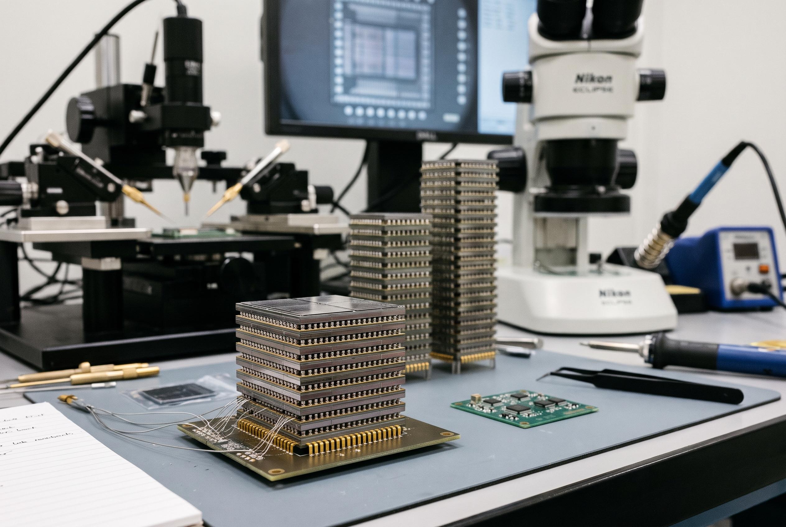

Manufacturing challenges are fuelling interest in eight-high and even four-high HBM, while hybrid bonding could be pushed back to later generations.
The race to build denser high-bandwidth memory is running into the practical limits of manufacturing. Although HBM has long been associated with ever taller stacks of DRAM chips, interest is now shifting towards lower-count products, especially eight-high configurations, as makers confront yield losses, heat management issues and packaging complexity in twelve-high HBM4. Some in the industry are even considering four-high variants, a sign that reliability and supply assurance are becoming as important as raw density.
That marks a notable change from the assumption that HBM4 would be defined by twelve-layer stacks. Samsung Electronics has already begun shipping HBM4 in a twelve-high format, while SK hynix has also been pursuing higher-stack development. Yet industry talk has increasingly centred on whether customers will accept a lower stack count if it improves production stability. The logic is straightforward: the higher the stack, the thinner the dies must be and the harder it becomes to bond them accurately without damaging yield or worsening thermal performance.
A lower stack count would not automatically replace twelve-high devices, but it could reshape how suppliers plan capacity and product mixes. NVIDIA’s Rubin architecture, which the company says uses twelve-high HBM4 and supports up to 288 gigabytes of memory with peak bandwidth of up to 22 terabytes per second, shows that leading AI platforms are still being designed around very high memory density. Even so, reports suggest that customers may not want to rely on a single stack height across all products. In that sense, the market may be moving towards a split approach, where different GPUs and different supply chains use different HBM formats depending on performance, cost and manufacturing readiness.
The change also has implications for hybrid bonding, the next-generation joining method that many in the sector once expected to arrive quickly as HBM stacks rose. SK hynix has described hybrid bonding as a direct copper-to-dielectric connection that can reduce package height, improve bandwidth and help heat transfer, but the company has also acknowledged the hurdles: yield, equipment capability and cost. Industry commentary has increasingly pointed to HBM4E or HBM5 as more realistic adoption points, rather than immediate use in current HBM4 production.
That delay matters for equipment suppliers. Hanmi Semiconductor and Hanwha Semitech both supply thermal-compression bonders to SK hynix, and if conventional stacking remains adequate for longer, those tools may stay relevant for a longer period than once expected. A slower transition to hybrid bonding would not necessarily hurt their near-term position. It could instead extend the life of existing bonding lines while the industry resolves the technical and economic barriers to a new process.
Behind the debate lies a broader issue: the AI memory market is growing faster than manufacturing capacity. One equipment executive said demand for AI memory is rising at nearly double-digit multiples year on year, while supply expansion is still trailing well behind. That means the answer may not lie only in stacking more chips. It may also require better system design, more efficient GPU-memory connectivity and software that uses memory more intelligently. As one academic observer put it, the industry now faces a choice between pressing on with taller stacks or improving the way the entire memory system is connected.
Disclaimer: This content is intended for informational purposes only. Readers are advised to exercise their own judgement, conduct due diligence, or consult a qualified expert before acting on any information provided.