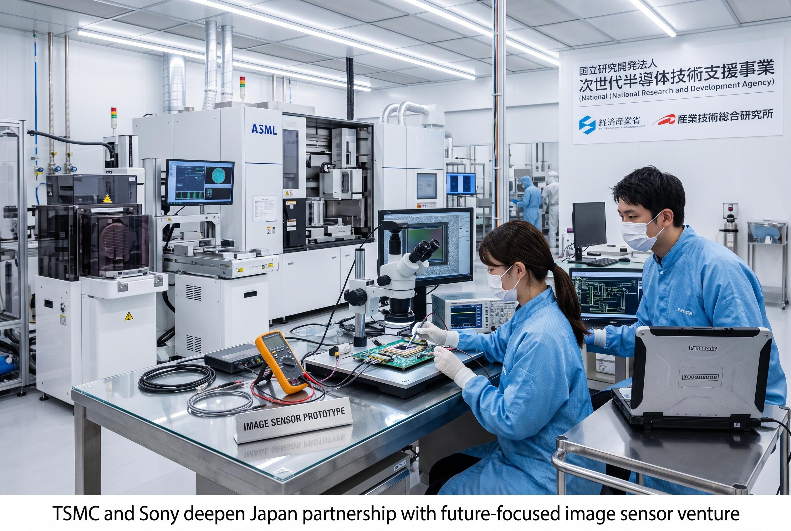

Taiwan Semiconductor Manufacturing Co. and Sony Semiconductor Solutions have formalised a joint venture in Japan, signalling a significant step in their collaboration on next-generation image sensors with commercial output expected by 2029, supported by Japanese government funding and expanding domestic chip production.
Taiwan Semiconductor Manufacturing Co. and Sony Semiconductor Solutions have moved from a preliminary understanding to a legally binding deal to form a joint venture in Japan for next-generation image sensors, a sign that the two companies are deepening a partnership built around advanced chip manufacturing and sensor design. According to reports from Focus Taiwan and Sony’s own announcement, the venture will be based in Koshi City, Kumamoto Prefecture, and will operate as a central development and production site for smartphone image sensors. TSMC said commercial output is planned for 2029.
Sony will be the controlling shareholder and will run the new company as a subsidiary of Sony Group. The representative director will be appointed by Sony Semiconductor Solutions. The ownership structure gives Sony operational control while allowing TSMC to contribute its process technology and manufacturing expertise, a division of labour that mirrors the companies’ existing strengths. Sony will handle product design, planning and core sensor development, while TSMC will provide advanced production know-how.
The financial commitment is substantial. Focus Taiwan reported that Sony Semiconductor Solutions plans to contribute about 465 billion yen, or $2.92 billion, through cash and asset transfers as part of a company split, while TSMC intends to invest about 282 billion yen. TSMC said those contributions will be phased according to market demand and broader business conditions, and that the plan assumes financial backing from the Japanese government.
The agreement follows a non-binding memorandum of understanding signed in May, which first outlined the proposed partnership. That earlier announcement said the venture would also look at applications in physical artificial intelligence, including automotive and robotics, reflecting a broader ambition than smartphones alone. Reuters reported at the time that the two firms were already discussing investment plans, subject to a definitive contract and standard closing conditions.
The new venture will also build on TSMC’s growing footprint in Kumamoto. Its first advanced fab in the prefecture began commercial production at the end of 2024 using speciality processes, and construction of a second plant began last year, with mass production using 3-nanometre technology expected to start in 2028. Together, the facilities reinforce Japan’s push to rebuild domestic semiconductor capacity while giving Sony access to manufacturing scale that is increasingly difficult to secure for cutting-edge image sensors.
Disclaimer: This content is intended for informational purposes only. Readers are advised to exercise their own judgement, conduct due diligence, or consult a qualified expert before acting on any information provided.