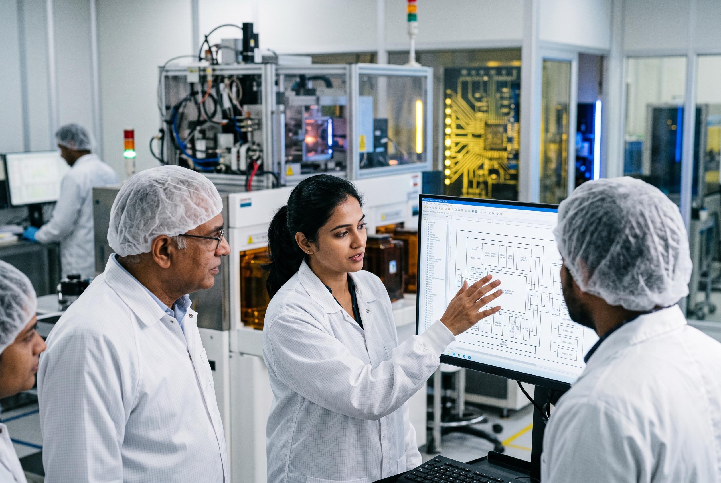

The Indian government plans a significant policy boost for chip design firms under Semicon 2.0, with a focus on scaling innovation, talent, and manufacturing capacity to accelerate the nation’s semiconductor ambitions.
India’s chip design startups are set to receive a bigger policy push as the government prepares Semicon 2.0, the next phase of its semiconductor mission, with Union electronics and information technology minister Ashwini Vaishnaw saying the state backing for design firms will more than double. Speaking at SEMICON India 2026 in New Delhi on 18 September, he said the shift would place deep-tech chip designers, as well as the country’s small manufacturers, at the centre of the sector’s next growth phase.
The new programme follows Semicon 1.0, which Vaishnaw described as the result of a longer-term strategy after decades of uneven policy attempts. According to the government, Semicon 2.0 has now been notified with an outlay of Rs 1,27,500 crore, and is built around six pillars: chip design, materials and equipment, additional fabrication capacity, more assembly, testing, marking and packaging units, research and development, and talent. Official documents say the scheme offers 40% capital support for silicon wafer fabs, while broader incentives also cover packaging, compound and display fabs, design support and ecosystem development.
Vaishnaw said the most startup-intensive part of the earlier phase was chip design, largely because access to electronic design automation software had been a major cost barrier. Rather than subsidising individual licences, the government pooled access through the Centre for Development of Advanced Computing, allowing young firms to work with the same tools used by larger chip designers. He said that approach helped more than 105 startups become chip design companies, and that around 20 of them later raised venture capital funding worth roughly Rs 800 crore. Under Semicon 2.0, the government is now targeting at least 200 chip design startups and companies.
The minister also tied the semiconductor effort to India’s wider precision manufacturing base. He said an industry executive at the event described exports of about Rs 2,000 crore, with nearly 90% of the supply chain coming from MSMEs. According to Vaishnaw, capabilities built for electronics assembly are already spilling into mobile phones, aerospace components and defence manufacturing. He also set out a stepped training model, beginning with a 240-hour introductory course and extending to higher levels of technical skill, alongside a planned Precision Manufacturing Institute. He said India had aimed to train 85,000 semiconductor design engineers over 10 years, with around 70,000 trained in the first four years, although recent government updates have also pointed to the full target being reached.
The next test will be whether that support can scale. Vaishnaw said the first wafer from Tata Electronics and PSMC’s plant at Dholera is expected in 2028, underscoring how much of the mission remains ahead rather than completed. For chip designers and the MSMEs feeding the sector, Semicon 2.0 will now be judged on whether shared infrastructure, talent development and capital support can turn early momentum into a broader industrial base.
Disclaimer: This content is intended for informational purposes only. Readers are advised to exercise their own judgement, conduct due diligence, or consult a qualified expert before acting on any information provided.