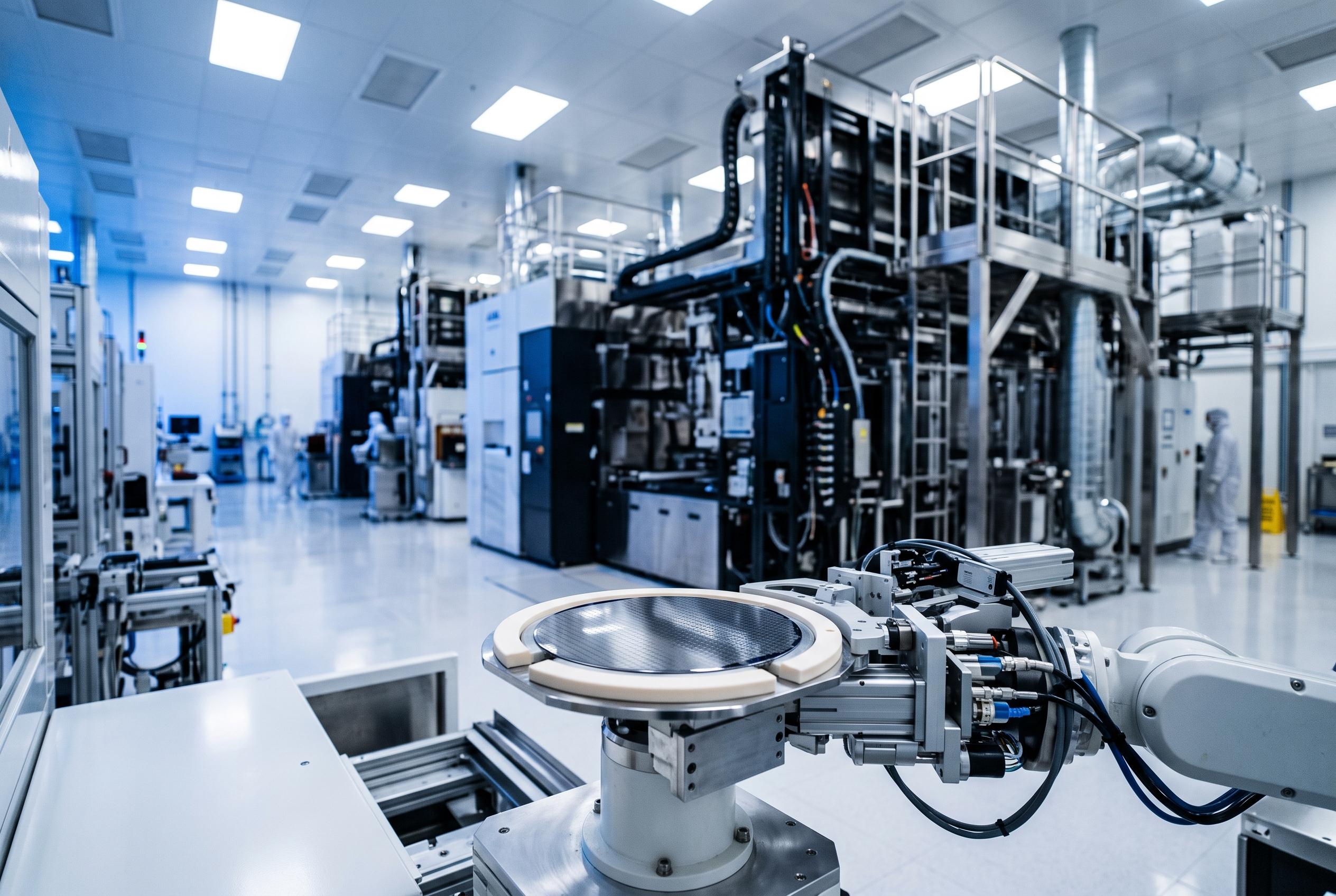

Intel has processed over a million 300mm wafers using High-NA EUV lithography, surpassing all other chipmakers combined and signalling a major industry transition towards larger photomasks and more efficient chip production.
Intel said on Monday that it has now run more than one million 300mm wafers through High-NA EUV lithography, a tally that it says exceeds the combined output of every other chipmaker using the technology. The figure covers tool qualification, research and development, and production work for its 18A process and Panther Lake processors, and it underlines how far Intel has pushed ASML’s next-generation scanners into regular manufacturing use.
The disclosure came alongside a broader shift in the industry’s position. ASML and TSMC announced an initiative on Sunday to move the sector towards 12-inch photomasks for High-NA EUV, with a pilot line targeted for 2031 and full system readiness for advanced-node production by 2033. Intel has backed the larger mask format for more than three years, but TSMC’s formal entry gives the effort wider industry weight and signals that the question is moving from a single-company campaign to a shared manufacturing programme.
The technical case centres on stitching, the workaround used when a chip is too large to fit within High-NA’s reduced exposure field. ASML’s High-NA scanners use an anamorphic optical design that halves the field height compared with current EUV tools, forcing large dies to be written in separate passes and joined with very tight alignment. That reduces throughput, adds cost and creates yield risk if the seam is not perfectly matched. Intel has already developed process-design-kit support for customers working within the current mask format, while ASML engineers are due to discuss stitching requirements at the SPIE conference in Monterey.
A move to 6×12-inch photomasks would restore the full exposure field and remove stitching altogether, but it would also require changes across much of the mask supply chain, including blanks, writers, inspection tools, pellicles, cleaning systems and handling equipment. ASML has not publicly said whether existing or planned EXE-series scanners can be adapted for that format. For now, the company and its partners are still working within the current 6×6-inch standard, even as the industry lays the groundwork for a larger one.
Intel’s scale matters because it has accumulated operational experience that rivals are still building. ASML said earlier this year that all High-NA systems shipped to customers had processed more than 500,000 wafers in total; Intel has now more than doubled that figure on its own. The company also says its Panther Lake parts made on Intel 18A with High-NA EUV on selected layers continue to meet performance targets. With TSMC planning High-NA high-volume manufacturing from 2030 and Samsung also working towards qualification, the next phase will be less about proving the technology works and more about deciding how quickly the industry can make it economically practical.
Disclaimer: This content is intended for informational purposes only. Readers are advised to exercise their own judgement, conduct due diligence, or consult a qualified expert before acting on any information provided.